
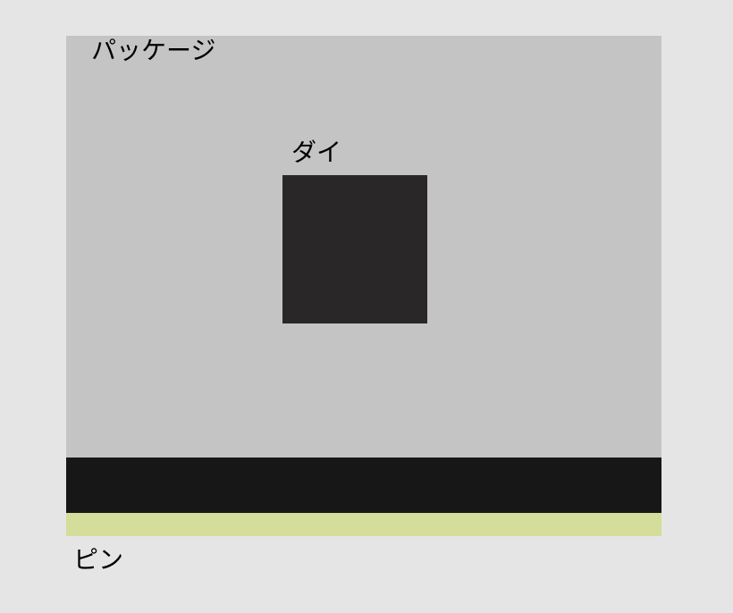
パッケージ:基盤
ダイ:集積回路、シリコンウェーハ(高純度シリコンから切り出された薄い板、ケイ素(Si))
ダイはバスインターフェイス、キャッシュメモリー、制御装置、演算装置からなる。
バスインターフェイス: 内部バス(CPU内部の回路)、外部バス(CPUとメモリ)
L アドレスバス、データバス、コントロールバスがある
キャッシュメモリ: バスメモリーから受け取ったデータを一時的に保存
L 一次キャッシュ、二次キャッシュ、三次キャッシュ
キャッシュメモリーがあれば、RAMにアクセスしなくて良いため、高速になる。
制御装置: フェッチユニット、デコーダー、レジスタ
L フェッチユニットは読み込み
L デコーダーはdecode
演算装置:整数演算ユニット、浮動小数点数演算ユニット、レジスタ
L 演算ユニットが複数ある場合、マルチコアとなる
L スレッドはOS(カーネル)が認識するコア数
ピンはCPUとマザーボードとの接続。LGA1151の1151はピンの数
最近のcpuでは発熱量に応じて、自動で電圧を上げて処理速度を高める設計
gpuがcpu内にあるものもある
あら、CPUの中に更にメモリがあるんですね。
Intel Core i7-4785T 2.2GHz Quad-Core SR1QU CPU Processor
Intel Core i5-4570T 2.9GHz SR1CA 5GT/s LGA 1150
Intel Core i7-6900K 20M Broadwell-E 8-Core 3.2 GHz LGA 2011-v3 140W
Threadripper 1950X YD195XA8AEWOF(AMD) 16コア、スレッド32
これはピンが4587個あるってこと?いや、違うな、型番か?LGAの後がピンの数ですね。
こうやってみると、i7-6900Kの8core 3.2GHzの性能が一番良さそうですね。
2.2GHzはクロック周波数。CPUはクロック信号に合わせて処理されるので、クロック周波数が大きい方が、高速になる。
ターミナルから確認できる
mac:ubuntu mac$ system_profiler SPHardwareDataType
Hardware:
Hardware Overview:
Model Name: MacBook Pro
Model Identifier: MacBookPro14,1
Processor Name: Intel Core i5
Processor Speed: 2.3 GHz
Number of Processors: 1
Total Number of Cores: 2
L2 Cache (per Core): 256 KB
L3 Cache: 4 MB
Memory: 8 GB
Boot ROM Version: MBP141.0169.B00
SMC Version (system): 2.43f6
Serial Number (system): **********
Hardware UUID: A7D32EAF-45A2-5CDD-AD44-**********
Number of Processorsが、1CPUで、total number of cores:2なので2コアという意味
AWSのvCPUはスレッドの方。
コア数とスレッド数の確認。logicalcpuの4がカーネルから認識されるコア数ということになる
mac:ubuntu mac$ sysctl -n hw.logicalcpu_max
4
mac:ubuntu mac$ sysctl -n hw.physicalcpu_max
2
カーネルは認識しているコア数(演算ユニット)に割り振って処理をする
CPUメーカーはインテル(シェア80%)、AMD(ゲーム用、キャッシュメモリが多い)
intelのcpu core architectの採用情報を見てみましょう
MS or PhD in CS, EECS, ECE, or related computing discipline
Minimum 10 years of experience with the following skillsets:
o High performance CPU microarchitecture and research
o Substantial experience with CPU simulators, tracing technologies, and performance analysis.
o Quick and efficient software development and debug skills
—-
In this position, you will be involving in the training, design and development of next generation SOC/CPU for wide range of Intel products. Your responsibilities will include some of the following but not limited to:
– Assist design unit owner in Register Transfer Level RTL model functional validation. Use CAD tool extensively to simulate logic behavior and circuit performance and direction of physical design for next generation, deep sub-micron embedded circuit solutions. Verify the circuit behavior against the original simulation model and first silicon.
– Define VLSI Structural Design methodology and developing design flows. Implement structural physical designs, such as synthesis, floor planning, power-grid and clock tree designs, timing budgeting and closure, place and route, RC-extraction and integration. Verify structural physical designs, such as functional equivalency, timing/performance, noise, layout design rules, reliability and power.
– Develop Analog IP on next generation deep submicron process for the Intel’s SOC, perform tasks related to Very-large-scale integration VLSI complementary metal-oxide-semiconductor CMOS IC design, Solid state physics and physical layout. Such tasks may include: Circuit design of high speed clocking related circuits [phase-locked loop PLL, delay-locked loop DLL, bandgap] or high voltage input/output IO [double data rate DDR/LPDDR, General-purpose input/output GPIO, OPIO].
– Responsible for Integration of Third party IPs — Synthesis, functional and/or timing convergence, and pre and post-si debug of IPs developed by various external vendors as well as within the company. Handling of signals crossing power planes and clock domains, industry standard protocols including hardware and software details dealing with Memory LPDDR, storage eMMC, SATA, UFS, peripherals PCIe, USB, and MIPI interfaces in SOC devices. System integration dealing with Si/ Platform/ FW/ MW/ drivers/ OS/ Apps on Android Windows-based tablets and phones.
Intel側はダイの設計をどうするか考えているわけだ。
すると、OSのカーネル側としても、クライアント側のcore数、スレッド数、GHzだけでなく、cpu内のキャッシュメモリ・GPUの設計なども意識して書いていくわけね。